
In this article, we will discuss center pads of Surface Mount Devices and their functions. Also known as a "Thermal Pad", the center pad is typically used for thermal dissipation which enhances the reliability and lifetime of the device. This is due to the fact that the die(s) typically sit on top of the thermal pad which provides a direct vertical path for heat extraction. The thermal pad of Luminus SMD packages is electrically isolated from the anode(+) and cathode(-) pads.
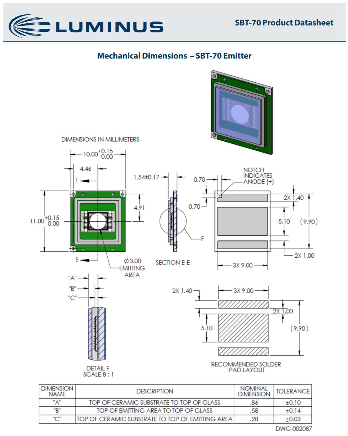
Below shows the Luminus SBT-70 pad device dimensions and the recommended solder pad layout. The SBT-70 is a high power SMD device. Using a circuit board layout that takes advantage of the thermal pad to spread the heat laterally will significantly improve the performance of this device.
Thermal Connections
We will use a simplified thermal model to illustrate the advantage of using a thermal pad to spread out the heat load in the top PCB copper trace. The figure below shows the model components.
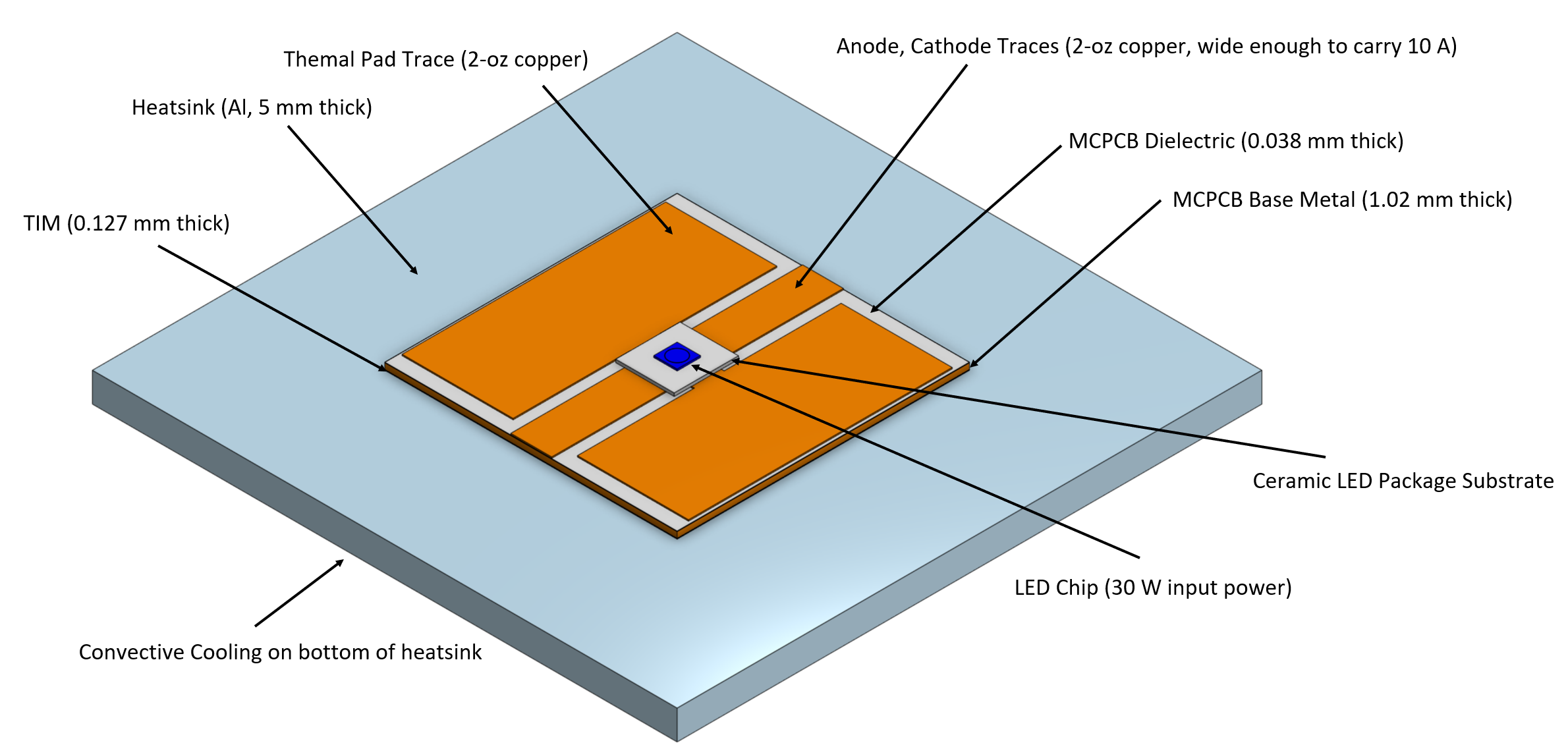
Thermal Model Layout
An LED chip is mounted on a ceramic substrate mounted on a printed circuit board (PCB) mounted on a thermal interface layer (TIM) mounted on a flat heatsink. Representative values for thermal and dimensional properties are used. Heat is introduced into the model in a 7 mm2 circular area on the top of the LED chip. Heat is extracted from the model at the back surface of the heatsink by convection (h=50 W/k-m2). The PCB is 50 mm x 50 mm and the heatsink is 100 mm x 100 mm. We will consider an applied power of 31 W in a 7 mm2 circular area (4.4 W/mm2).
We examine changing two variables, the base material of the PCB (copper, aluminum, FR-4) and the "connection" to the thermal pad. Connection condition 1 has the thermal pad connected to the 2-oz copper trace as shown above and condition 2 simulates a disconnected thermal pad by changing the thermal conductivity of this PCB trace to 0.001 W/m-K.
Model results are summarized in the table below.
| PCB Material | Thermal Pad | Tj (C) | T_hs (center) | T_hs (Edge) |
| Copper | Connected | 127 | 89 | 83 |
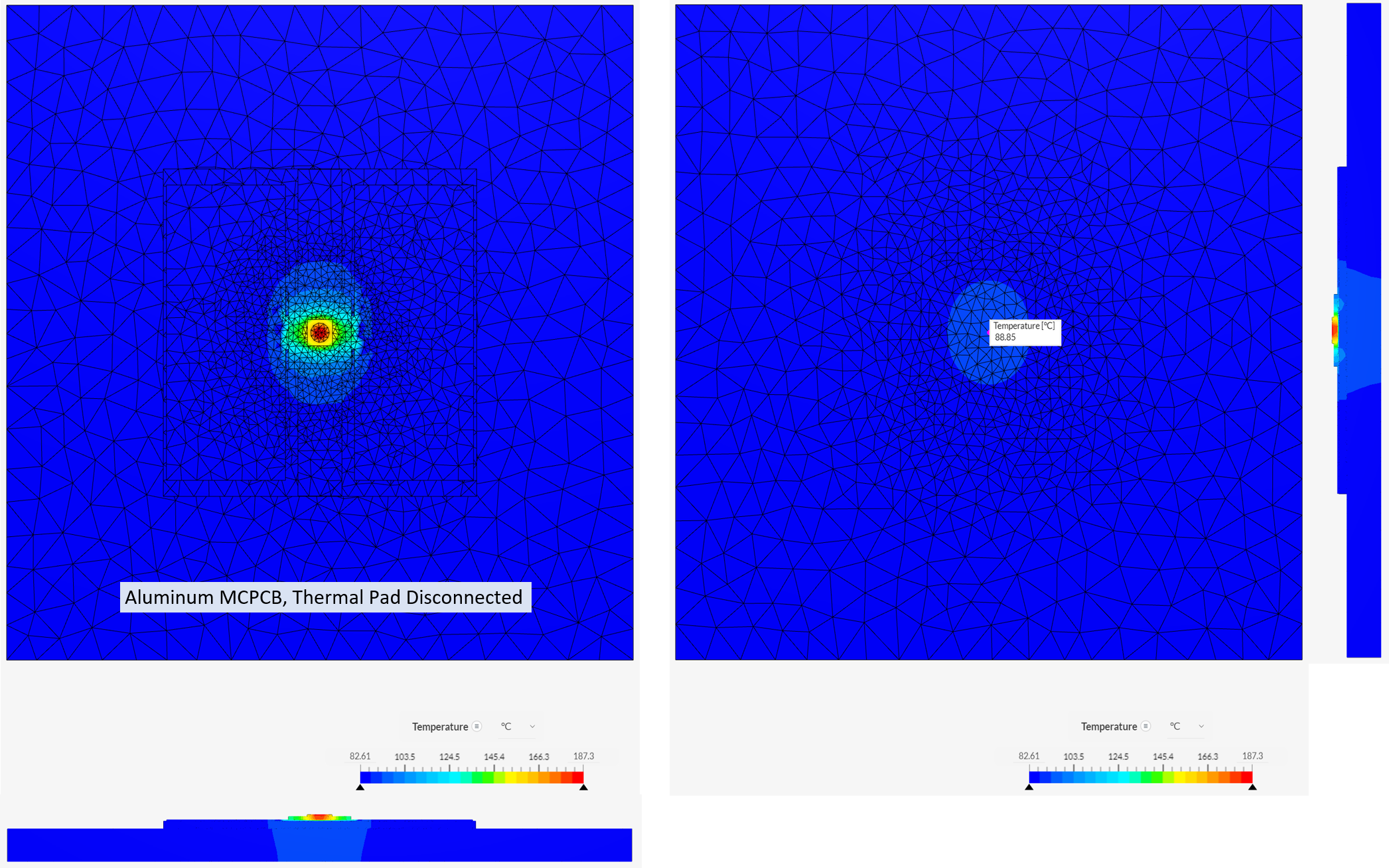
| Aluminum | Connected | 130 | 89 | 83 |
| Copper | Disconnected | 186 | 88 | 83 |
| Aluminum | Disconnected | 187 | 89 | 83 |
| FR-4 | Connected | 198 | 87 | 83 |
| FR-4 | Disconnected | 325 | 88 | 83 |
These results are for a simplified model to illustrate heat spreading effects and do not include all of the heat extraction mechanisms for this type of system. The FR-4 model is particularly suspect. Adding convective cooling to the top of the FR-4 model is needed to get a better approximation of the thermal profile.
This model simplistically forces 31 W of power to flow in through the LED chip and 31 W of power to flow out through the bottom of the heatsink and calculates the thermal profiles between these boundary conditions using the thermal conductivity and geometry of each layer. The bottom of the heatsink has to have an average value near 85 C to achieve energy balance with the arbitrary values of h and A used for this convective cooling model.
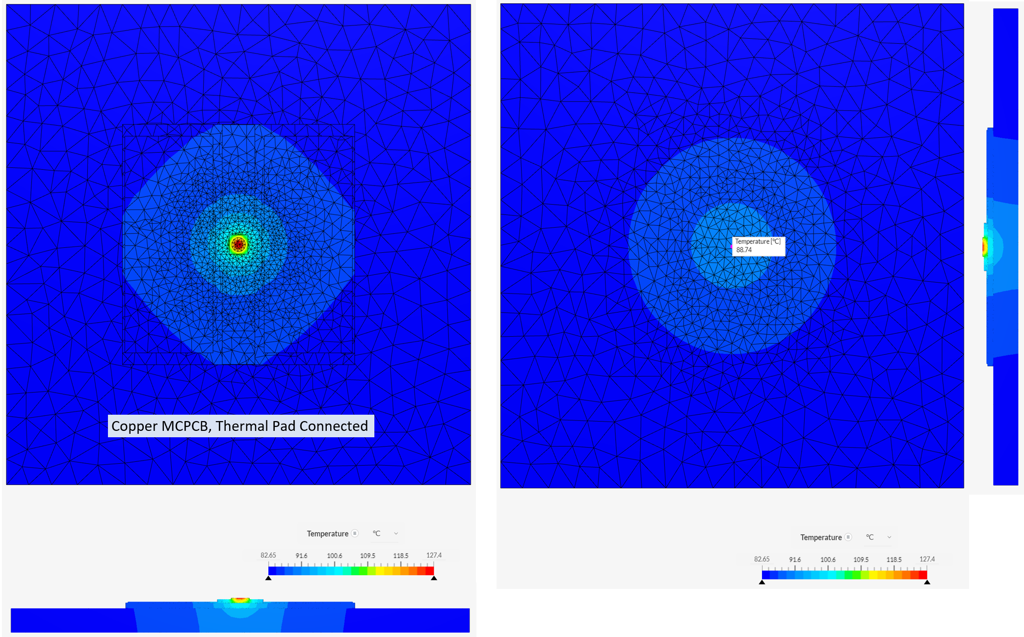
This all copper configuration has good heat spreading. The 2-oz copper traces on the top layer and the copper base of the MCPCB provides the best case for thermal spreading.
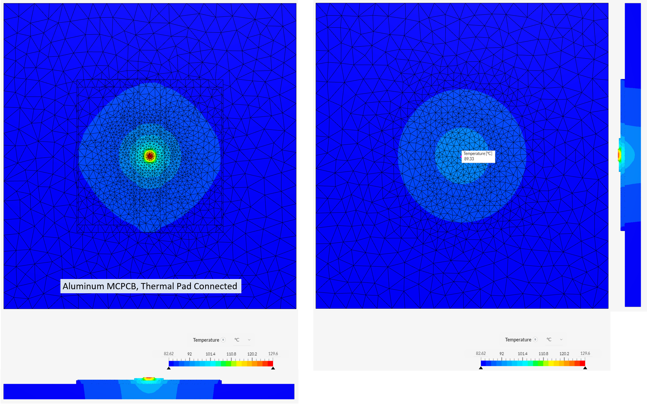
This configuration also has good heat spreading. Aluminum and copper MCPCB base metals have similar performance. The copper MCPCB Tj is 2.3 percent better than the aluminum MCPCB Tj in this model.
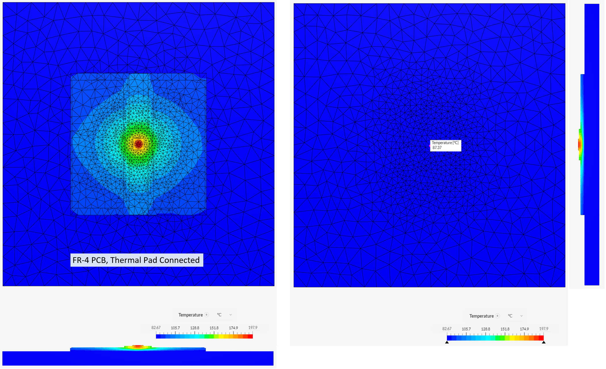
This configuration has good heat spreading in the 2-oz copper metallization on the top layer of the PCB but the vertical heat flow is poor due to the low thermal conductivity of FR-4. The junction temperature is well above the safe limit of 150 C due to this thermal choking.
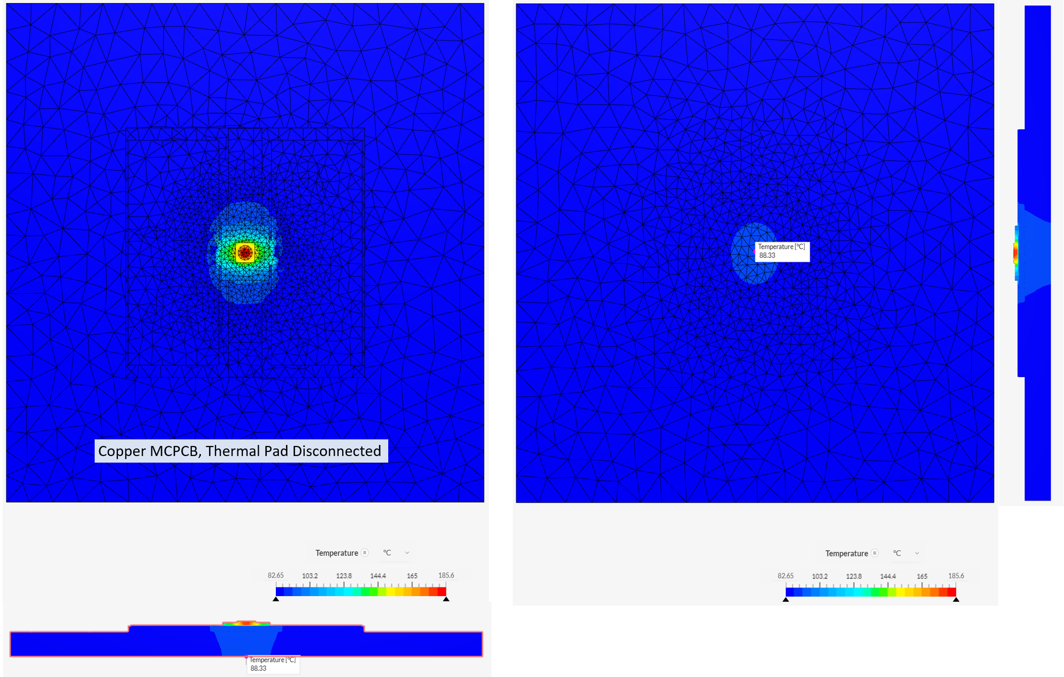
Disconnecting the thermal pad causes poor heat spreading. The junction temperature is now well above the safe limit.
Basically the same result as the all copper configuration. If you zoom in, you can see the heat flow from the anode and cathode in the side cross sectional view.
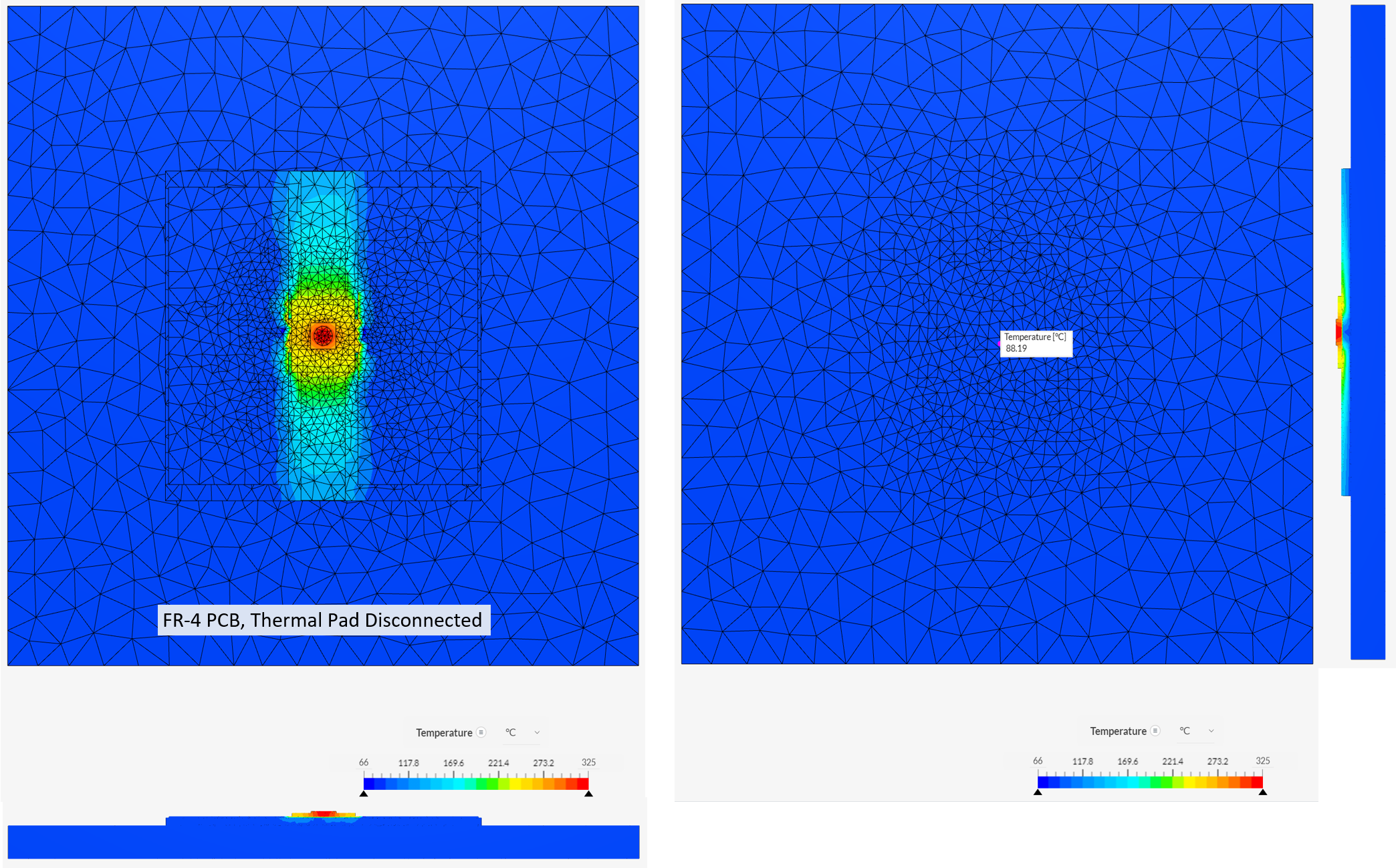
This model has failed. The predicted junction temperature is above the melting point of solder so this condition cannot physically occur.
Optical Efficiency
The power applied to this model is thermal. It is not the same as the power applied to the LED (I * V) because a significant fraction of that power leaves the system as light. The optical efficiency of the
SBT-70-B at the test point is calculated as:
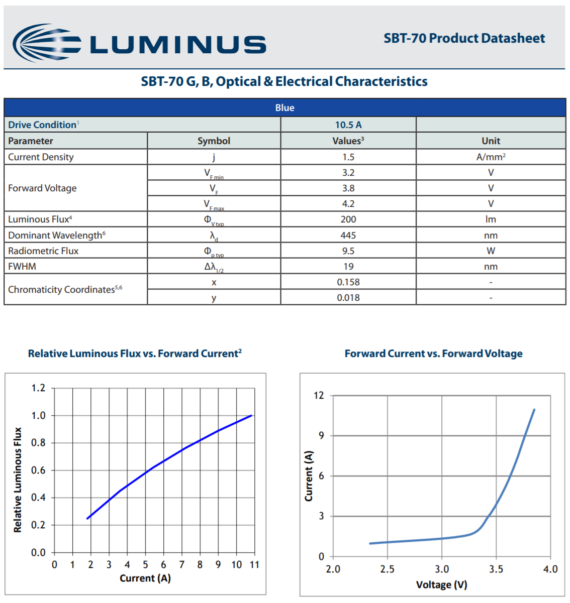
Electrical Power Input = I * V = 10.5 A * 3.2 V = 33.6 W.
Optical Power Out = 9.5 W.
Thermal Power In = 33.6 W - 9.5 W = 24.1 W.
Optical Efficiency at the test point = 9.5 W / 33.6 W *100 = 28.3 %.
The optical efficiency is a function of drive conditions. It can be calculated for different conditions using the charts in the datasheet.
Electrical Connections
The thermal pad for Luminus SMD devices is electrically isolated. It can be
- Left floating
- Connected to the system ground
- Connected to the anode(+)
- Connected to the cathode(-)
Luminus recommends connecting the thermal pad to the cathode(-). This ensures that the voltage between the anode(+) and the combined thermal pad/cathode(-) is the voltage across a single LED. Note that if there are a number of LEDs in the board layout connecting all of the cathodes (-) to one copper pour will short out the intended design.
Connecting the thermal pad to ground will make the voltage between each anode and cathode in a string with respect to the thermal pad be the same as the voltage difference to ground. In a high voltage series configuration, this may cause problems.
Leaving the thermal pad floating will most likely have no deleterious effects, but the voltage of the floating pad is uncontrolled and subject to capacitive charging from the rest of the system.
Multiple pad layouts
Some Luminus devices, such as the SBM-40 feature a multi-pad layout. In these cases there will be multiple cathode and anode assignments on the package. Please refer to the related product datasheet for the correct pin-out locations. The pad in the center that is unmarked will function in the same manner as 3-pad designs where the function is primarily for the optimal thermal path.
In designs utilizing these devices, it is strongly recommended to leave the thermal pad floating or connected to ground, as connecting this pad to the electrical pads may cause problems during the operation of the device.
--------------------------------------------------------------------------------------------------------------------
Luminus Website https://www.luminus.com/
Luminus Product Information (datasheets): go to the main page and select Products and then select the type of product you are interested in.
Luminus Design Support (ray files, calculators, ecosystem items: [power supplies, lenses, heatsinks]): go to the main page and select Resources & Tools and select the item you are interested in.
Luminus Product Information sorted by Applications: go to the main page and select Applications.
Where to buy Samples of Luminus LEDs: https://www.luminus.com/contact/wheretobuy.
--------------------------------------------------------------------------------------------------------------------
Technical Support Contact Information: techsupport@luminus.com
Sales Support Contact Information: sales@luminus.com
Customer Service Support Contact Information: cs@luminus.com
Comments
0 comments
Please sign in to leave a comment.