
(HC-211014)
Reflow soldering SMD components has a large number of variables: type of solder, particle size and flux, component density and circuit board mass, solder paste printing details, reflow equipment used, to name a few. It is not possible to provide a single solution that covers all applications. Luminus recommends using the solder paste manufacturer’s’ instructions as a starting point in process development. Below, we provide a set of best practice guidelines.
Luminus recommends using an SAC305 solder paste with a no-clean flux for RoHS compliant products. A properly activated no clean flux leaves some visible residue that have no long-term deleterious effects on reliability. Cleaning the circuit board is not required, but if desired, isopropyl alcohol and DI water may be used. Ultrasonic cleaners or vapor degreasers are not recommended and may damage the device. Do not use acetone or any type of acid.
Apply solder paste to the PCB with a screen or stencil using a thickness range of 0.15mm (0.006”) to 0.25 mm (0.010”). Luminus recommends you locate the equipment in a controlled environment maintained at a temperature of 23 ± 5C and a relative humidity less than 60%.
The reels supplied by Luminus are ready for automated pick and place operations. We recommend that manufacturers automate the solder paste printing process by using a pick-and-place machine with an integrated stencil print cell. If this is not an option, solder paste printing can be completed manually as an offline process.
The figure below shows an example of the dimensions of the tape for a Luminus LED component and the orientation of parts within the reel. Industry standard “cathode towards the holes” orientation is used. Further information can be found in the respective product datasheets.
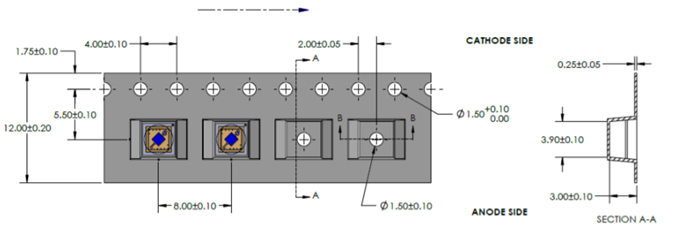
Example of tape dimensions and device orientation provided in the datasheet.
The figure below shows the orientation identification markings for individual components. The middle pad is the thermal pad, further discussed in this article. Luminus maintains a database of electronic design files in collaboration with SnapEDA. Symbols and footprints are available in a wide variety of formats including Altium, Eagle, Pads, OrCAD, and more. Access to these files online will allow designers to incorporate Luminus products into circuit designs without having to spend time creating the library files. 3D step files are available for download as well.
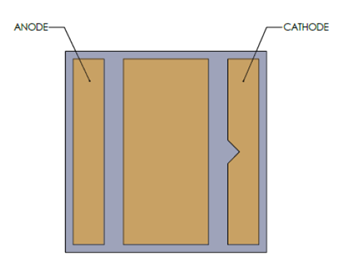
Example of an orientation mark in a Luminus SMD component.
Luminus recommends using a vacuum pick-up tool for the pick and place of surface mount products. Exercise care when handling the devices. For example, sudden forces on the dome or window, such as those caused by dropping the device on a hard surface, may damage the device. During the pick and place process, axial forces on the dome (or window) should not exceed 0.5 Newtons (N).
A variety of pick and place nozzles can be used. Since pick and place equipment is not standardized, it is not possible to give a single part number as a recommendation. Established operations will probably have a suitable nozzle on hand or already know where to source one. For new operations, we recommend consulting Small Precision Tools (SPT). Luminus collaborates with SnapEDA for online storage of SMT footprint and 3D model data files. More information can be found here. There are a variety of materials that can be specified for pick and place tools (metal, polymer, Teflon). All of these have been successfully used in mass production after factory process development.
Use of a multi-zone IR reflow oven with a nitrogen blanket is recommended. Adjustable heating zones gives more flexibility in developing thermal profiles with high throughput. Nitrogen blankets allow the use of less aggressive fluxes, which will improve reliability, and eliminates the possibility of sulfur damage during the high-temperature reflow spike (the environment often contains low level sulfur sources such as solvents, paper, and rubber). When using copper-based MCPCBs, a nitrogen blanket will prevent oxidation of the copper base material.
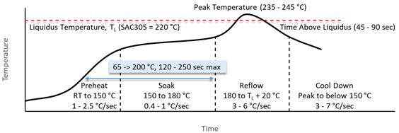
Time-temperature profile of the reflow process showing the four functional profile zones defined in
IPC-7801. Temperature is referenced to the center of the PCB. Typically this is done by gluing a thermocouple to a test panel and then either using a temperature resistant data logger or spooling wire through the system to record the temperature as the PCB moves through the reflow oven.
Slight increases in the peak temperature needed to get good results are unlikely to damage the LED component but are a symptom of too fast of a ramp rate before the reflow spike. The PCB has not preheated enough for the solder paste manufacturer's recommended spike temperature to be effective. This can also cause excessive voids which is a significant root cause of premature field failure for all types of SMD components including LEDs.
Reflow Profile Rate Optimization
|
Profile Zone |
Too Fast |
Ideal |
Too Slow |
|
Preheat |
Solvent Evaporates too fast - Solder Balls, Voids Have to use a high temperature spike in the reflow step. |
Excess Solvent Evaporates |
Hot Slumping - Solder Bridges |
|
Soak |
Solvent Evaporates too fast - Solder Balls, Voids Have to use a high temperature spike in the reflow step. |
Flux Starts to Activate and Reduces Oxides on all Metal Surfaces |
Hot Slumping - Solder Bridges |
|
Reflow |
Insufficient Heat - Cold, Grainy Solder Joint, Incomplete Melting (balls) |
Solder Paste is brought above Liquidus |
Excessive Heat - PCB Discoloration, Leaching |
|
Cool-Down |
Thermal Shock - Component Damage |
Even Cooling - No damage |
Excessive Intermetallic Formation |
Luminus recommends performing X-ray inspection during reflow process development with an acceptance criteria for solder joint quality as Cpk > 1.25 (or 1.60) for void count percentage using a 20% single-sided limit. Establishing an SPC sampling plan for X-ray inspection during mass production is recommended.
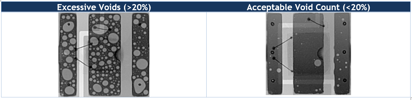
Examples of X-ray void characterization during LED reflow process development.
--------------------------------------------------------------------------------------------------------------------
Luminus Website https://www.luminus.com/
Luminus Product Information (datasheets): https://www.luminus.com/products
Luminus Design Support (ray files, calculators, ecosystem items: [power supplies, lenses, heatsinks]): https://www.luminus.com/resources
Luminus Product Information sorted by Applications: https://www.luminus.com/applications
Where to buy Samples of Luminus LEDs: https://www.luminus.com/contact/wheretobuy.
--------------------------------------------------------------------------------------------------------------------
Technical Support Contact Information: techsupport@luminus.com
Sales Support Contact Information: sales@luminus.com
Customer Service Support Contact Information: cs@luminus.com
Comments
0 comments
Please sign in to leave a comment.